DDS AD9850 with PLL FS6370 Clock generator
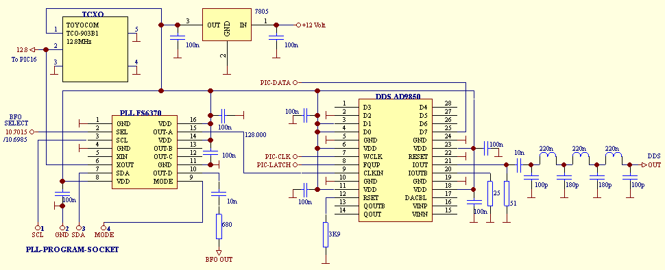
Data, Latch, and Clock from PIC16 CPU, to control the DDS counter value of 32 bits.
The USB/LSB bit is also controlled by the PIC
The PLL Needs to be programmed only one time during development, it contain an EEPROM so that it will startup with the right values
The 128Mhz main clock, comes from a PLL IC called FS6370 (look at bottom of this page)
it's 3 PLL's and VCO's and all the counters dividers loop filters multiplexers in one little 16 pin smd pakage
The DDS spec. says 125 is max. but 128 is only 2.4% more, I am sure this will work for you all..
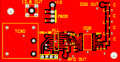
The NEW PCB, only top layer is shown, Download Gerberfile
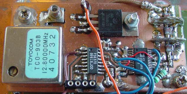
The new board with TCXO, PLL, and DDS. Note the two "walls" mounted to shield the output filter coils.
The 7805 Regulator seem really BIG compared to the small chips.
DDS output Filter

The output from the DDS needs to be filtred, before entering the DDS amp.
Look here to see how to make a 220nH coil for the filter
IOUT of the DDS has about 2 Volt DC offset, This output need 50 Ohm resisive load to minimize spurius
The Math behind the DDS chip:
Fout = Word / 2^32 x FclockResulution = Fclock / 2^32
Word = Fout / Fclock x 2^32
The BFO USB frek is 10.7015
DDS word    DDS frek     RX frek:
828844802 = 24.701.500 = 14.000.000
840588853 = 25.051.500 = 14.350.000

828844802 / 24701500 = 33.554432

So the trick is to multiply the frek in hz with 33.554432 this can be done with the PIC at only 1.2mS
The DDS 128 Mhz Clock
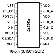
Here is the pinout if the PLL IC FS6370, See the block diagram
This IC is Three EEPROM- programmable phaselocked loops (PLLs) driving four programmable muxes and post dividers
provide a high degree of flexibility. As shown in Figure, each PLL consists of a Reference Divider,
a Phase- Frequency Detector (PFD), a charge pump, an internal loop filter, a Voltage- Controlled Oscillator (VCO), and a Feedback Divider.
More info about FS6370
The PLL IC gets it input refference frequency from the 12.8 Mhz TCXO that also feeds the PIC with clock
Output A is programmed to give 128.000 Mhz exactly 10 times the input clock, but now the 128Mhz is not multiplied up to the desired frequency but PLL'ed
This has several advantages: any small drift is not also multiplied, say: if the refference goes 10Hz up, the 128Mhz will also go 10Hz up
If the 128Mhz was multiplied it would have gone 100Hz up !
Also the 128Mhz is generated in a VCO that is voltage controlled via a loopfilter that make sure that the phase noice is at a minimum
Now the best part: Output B is programmed to generate 10.7015 Mhz (the BFO freq for USB) this is also locked to the same stable TCXO !
The difference between VCO and BFO is the recieved and transmitted frequency, this difference is made DIGITALY via the DDS
so now it's not possible to have any frequency drift at all !!
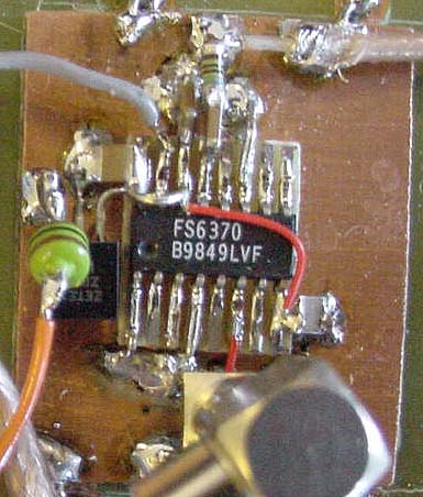
Here is a close up of the FS6370 PLL test setup
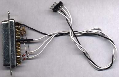
A simple adapter connected to my scanner cable that goes into the PC parallel port
Connect like in the datasheet but don't connect the SEL and +5 volt.
Now the windows program downloaded from AMI web site can easy configure the PLL to give out the right frequencies
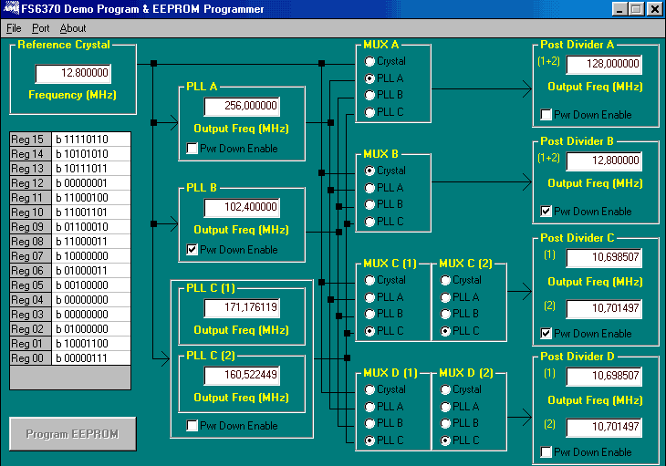
The PLL A runs at 256 Mhz and is divided by 2, this gives 128 at 50 % duty cycle, and halves eny drift
The PLL B is selected to have powerdown enabled, this will shut it off, also output B and C are shut off
PLL C has (1) and (2) values depending on the input pin SELECT, At output D the dividers has (1) and (2) options that will make the BFO output 10.7015 and 10.6985
The small error of 30Hz is also calculated with in the PIC software that controll the DDS
The DDS output Amplifier
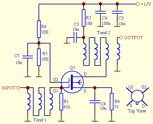
The output of the DDS is not powerfull enough to drive the Mixer so a gain of 10 db is needed
This amp is now made broadband so that it can be used on all bands to generate the first mixer signal, from 14 to 40Mhz.
The two toroids is 9.4 x 5.5 x 3.4mm, made by Ferroxcube, Order Code = 432202097170, material = 4C65, AL value = 30, Core is purple.
The 3 and 4 cores 0.15mm Cu, is twisted good before making the 5 turns.
If another frek range is wanted, change the turns: 10 turns for 2-30Mhz, 5 turns for 13-50Mhz.

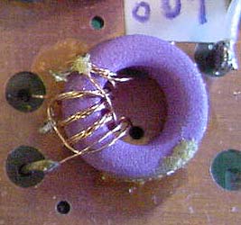
To test if a core can be used, take an unknown core of the right size, add 10 turns one Cu wire, if right material the inductance will be about 3 to 3.5 uH
If you can not measure the inductance, mount a 100pF capasitor in parallel with the coil, now measure the resonans frequency, if right coil the freq will be about 9 Mhz
But remember to calculate with the capasity in the scope probes, some have 10 to 20 pF, so in real life total capasity will be 140pF and the resonans freq will be about 7 Mhz