AP2000 UHF Technical description
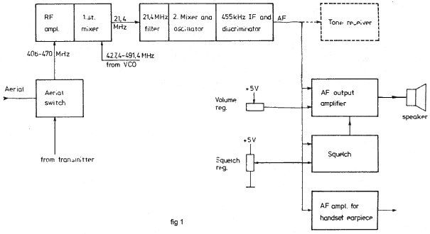
RECEIVER (FIG. 1)
Aerial Switch dwg. no.75624-4E2
(for sets with ext. PA see dwg. no. 75627-4E2)
The aerial switch is made by a relay, while TR 1 D 1 and D 2
makes a forward power sensing circuit for the transmitter.
This circuit is used for power regulation.
-----------
RF-amplifier and 1st mixer (75476-4E2)
The RF-amplifier consists of a bipolar transistor with several
tuned circuits, of this 4 helicoils, to give the necessary selectivity.
This first mixer converts the RF-signal 406-432 MHz or 450-470 MHz to 21,4 MHz
with an oscillator injection of 427,4-453,4 MHz respective 471,4-491,4 MHz on the gate.
Matching of the mixer output impedance to the crystal filter is made by the tuned circuit L 6.
-----------
21,4 MHz and 455 kHz IF (75076-3E2)
The 21,4 MHz crystal filter is followed by a dual-gate Mos-amp-
lifier which gives approximately 20 dB gain. This stage is follo-
wed by the second mixer which converts 21,4 MHz to the low IF 455
kHz. The second mixer consists of an integrated doublebalanced
transistor mixer, in which one section is used as the crystal osc-
illator. An emitter follower with some RC low-pass sections feeds
the signal to IC 2, which is an integrated high gain amplifieri
limiter and quadrature detector. The coil L 4 is the detector pha-
se shift network. AF output is supplied by the emitter follower Q 3
------------
AF-amplifier, squelch and key circuit (75017-3E2)
The AF-signal goes through an amplifier stage Q 6 to the volume
control circuit. Here, the diodes D 1, D 2 and D 3 act as an
electronic attenuator regulated by the diode current. This cir-
cuit is also used for external AF-blocking and squelch. An inte-
grated AF output amplifier is used for the 3 W loudspeaker output
and here the feedback-capacitors C 6 and C 7 produce the
deemphasis for the handset earpiece Q 4 and Q 5 gives the amplification.
The squelch circuit consists of an 8 kHz tuned amplifier Q 3
followed by a detector D 11 and D 12. With increasing noise level on the
AF-input the voltage on the negative side on C 19 will decrease
from + 5 V. Getting lower than the squelch reg. voltage on point
7, the amplifier IC 2 switches over to an output voltage of + 5 V
and thus blocking the AF-output through the volume control circuit.
In the key control circuit Q 1 and Q 2 goes ON when the button in
the handset connects point 11 to chassis, thus producing + 12 V
on point 14. A positive voltage applied on point 10 will inhibit this function.
----------------
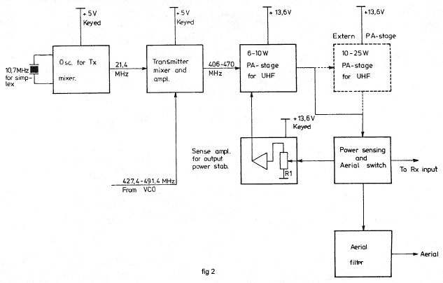
TRANSMITTER ( FIG. 2)
Transmitter mixer and amplifier (75511-4E2)
Because the VCO has a freguency 21,4 MHz higher than the operating
Rx-frequency this is fed to the transmitter mixer and converted
to the desired transmitting frequency. For simplex operation the
necessary 21,4 MHz signal comes from a vombined crystal oscillator,
doubler (75628-3E2). Thus the crystal will be 10,7 MHz. For good
suppression of VCQ - and 21,4 NHz injection the Tx-mixer is a bal-
anced transistor type. The two amplifier stages Q 3 and Q 4 give
further suppression of unwanted sidebands and necessary amplifica-
tion to reach an output of approx. 30 mW.
----------
6-10W Power amplifier (75510-4E2)
This power amplifier consists of three stages Q 1, Q 2 and Q 3,
where the output level can be regulated by varying the supply vol-
tage for Q 1 and Q 2. The regulation voltage is taken, from the
forward power sensing circuit. Situated on print board B 58 C 1.
------------
10-25W PA-stage (75627-4E2)
This amplifier consists of one stage Q 1, and is driven from the
6-10 W amplifier. The output of Q 1 goes through a forward power-
sensing circuit to the aerial switch. The output is adjustable
with R 2.
------------
Output power stabilizing (76325-4E2) and (75622-4E2)
From the power-sensing a DC voltage proportional to the forward
power is led to an amplifier. Here it is compared to a zener-
voltage, and if it is greater than this threshold level, the
amplifier IC 1 will give a lower output voltage for the supply of
Q 1 and Q 2 (75510-4E2), thus reducing the drive level. This
will act in the following manner:
For low supply voltage (~ll V) the output power will increase
with increasing supply voltage, and when the output reaches the
desired value it will be constant for further increase in the sup-
ply voltage. The output level for supply voltages greater than
approx. 13 V is adjustable with R 2 on print board B 59 for power
outputs between 10-25 W and R 1 on print board B 57 for power
outputs between 6-10 W. Note that the oscillator for Tx-mixer,
the transmitter mixer and amplifier, and sense amplifier have
keyed supply lines, while the final transistor in the 6-10 W stage
and the 10-25 W stage are supplied independent of the key.
------------
Aerial filter (75623-4E2)
The aerial filter is a low-pass filter for suppression of the
harmonics from the transmitter.
------------
Modulation amplifier (750l8-3E2)
The modulation amplifier has a preamplifier Q 1 for the most sen-
sitive input (input 1). Using the less sensitive input 2, the
Mic. switch terminal shall have + 5 V so that Q 1 will be block-
ed via D 3. D 4 will be conducting and feed the AF-signal to IC 1.
For selective tone transmission the tone Tx input is used while
Q 1 is blocked via D 2. D 5 is used for blocking of the modulation
amplifier while receiving in simplex mode. IC 1 and the first
part if IC 2 work as a compressor/amplifier to limit the maximum
output AF-voltage. When using a variable gain type amplifier as
IC1 it is possible to avoid the distortion for high AF-levels,
which occurs in a conventional clipper-circuit. The other ampli-
fier in IC 2 is used as a 3 kHz active low-pass filter. A tuning
diode in the VCO is used for modulation.
-----------
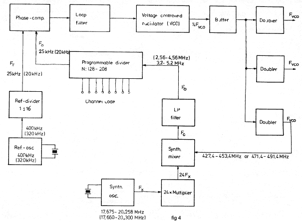
The synthesizer circuit in AP 2000 (Fig. 4)
Synthesizer logic (75062-3E2 25 kHz and 77201-3E2 20 kHz)
The 25 (20) kHz reference frequency is produced by dividing a 400
(320) kHz crystal oscillator (X 1 and Q 4) by 16 in the counter IC6
The output signal to the programmable divider is amplified in
Q 1 and Q 2, while the two gates from IC 1 shape the waveform to
narrow pulses. IC 2 and IC 3 form the programmable divider, where
the division ratio N is the binary number on the eight channel
code lines. The numbers on the codes lines correspond to the
binary value of each line. In this way a division ratIo N = 168
will have a channel code:
Number on code line 128 64 32 16 8 4 2 1
Binary value 128 64 32 16 8 4 2 1
Code for N = 168 1 0 1 0 1 0 0 0
where 0 means 0 V and 1 means + 5 V.
The two cascaded counters IC 2 and IC 3 count down from 168.
When the counters reach zero a borrow pulse is generated and
used to preset the number 168, thus starting a new count cycle.
The very narrow borrow pulses with a repetition rate of 25 (20)
kHz are used as input to the frequency-phase comparator IC 4.
The comparator output voltage V1 (Fig.2) can be seen on a test
point TP 1. To suppress the 25 (20) kHz ripple on the compara-
tor output voltage Q 3 is connected as an active lowpass filter
IC 5 is for DC-amplification.
----------
Voltage controlled Oscillator (76024-3E2)
The transistor Q 2 is used to switch between two loop filters.
When Q 2 is '0N' the slow filter R 1, R 3 and C 15 are in func-
tion while R 1, R 2 and C 16 give the loop a fast step response
for Q 2 '0FF'. The fast loop filter is only used in connection
with automatic channel scanning. Diode D 2 is used to clamp the
control voltage thus preventing too great VCO frequency excur
sions when the loop is out of lock. The frequency of oscillator
Q 1 is controlled by tuning diode D 3 while diode D 4 is for
modulation. To avoid excessive loading of the oscillator it is
followed by a wideband bufferstage Q 3. Transistors Q 4 to Q 6
make the three output multipliers with tuned collector circuits.
-----------
Synthesizer mixer ( 75628-3E2)
In the synthesizer mixer Q 1 and Q 3 act as a combined crystal
oscillator/doubler. Since the crystal frequency is about 20 MHz
and the tuned circuits L 1 and L 2 are tuned to the second har-
monic of the 40 MHz collector frequency, the input frequency to
the mixer Q 4 is about 80 MHz. The VCO-signal goes through the
dual gate Nos-transistor buffer Q 2 which gives high backward
isolation but no amplification. Reaching the base of Q 4 the VC0-
signal is mixed with the sixth harmonic of the 80 MHz to give an
output signal of 3,2 - 5,2 (2,56 - 4,56) MHz. L 5 and L 6 are part
of a 10 MHz low-pass filter connected to the amplifier stage Q 7.
-----------
Channel code
From the blockschematic of the synthesizer circuit (Fig. 4)
we have:
Fvco = 24 Fx + N x 0,025 (0,020) MHz where 128 N 208.
The VCO frequency lies 21,4 MHz above the receiver frequency
leading to:
Reciever frequency Fm = 24 Fx + N x 0,025 (0,020) - 21,4 MHz
Here N is the division ratio and F is the synthesizer mixer
crystal. Fx is found from the drawings 75499-4E2, 75500-4E2
and 76132-4E2. For a single channel set you can choose between
two standard crystals beeing equally good. Considering a multi-
channel set, in most cases only one standard crystal will fit
the desired frequency range.
------------
1. Computation examble of the receiver frequency for 25 kHz set:
Known is: Crystal frequency Fx and channel code.
Example: Fx = 19,675 MHz
Code: 1 0 0 1 0 0 1 1
Division ratio N = 128 + 16 + 2 + 1 = 147
Using equation (5):
Frx = 24 x 19,675 +(147 x 0,025)- 21,4 = 454,475 MHz
2. Coniputation of the channel code:
Known is: Crystal frequency Fx and desired receiver frequency Frx
Rearranging equation (5) gives
Frx - 24 Fx + 21,4
N = --------------------
0,025
Example: Fx = 19,675 MHz, Fx = 455,625 MHz
N = (455,625 - 24 x 19,675 + 21,4) /0,025 = 193
N = 128 + 64 + 0 + 0 + 0 + 0 + 0 + 1
Channel code = 1 1 0 0 0 0 0 1
NOTE: Because of the special synthesizer oscillator circuit, it has
been necessary to specify the crystal Xl with a parallel capacity of
l5pF. If you use a crystal specIfied with 3OpF parallel capacity, the
frequency should be about 250 ppm lower than the standard frequency
given on the drawings 75499-4E2, 75500-4E2, and 76312-4E2.
Exactly the same procedure is used when the set is intended for 20
kHz channel spacing.
------------
DIVISION RATIO AND CHANNEL CODE
The division ratio N corresponds to the 8 - bit
channel code in this way.
Bit number 8 7 6 5 4 3 2 1
Value of each bit 128 64 32 16 8 4 2 1
Example: channelcode 1 1 0 0 0 0 0 1
N = 193 = 128 + 64 + 0 + 0 + 0 + 0 + 0 + 1
Logic 1 = +5 Volts. Logic 0 = 0 Volts
Division ratios must be from 128 to 255
Divions under 128 vil generate to low ref freq
and this will make PLL locking impossible
-------------